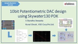
VSD Intern – DAC IP design using Sky130 PDKs – Part 1
Learn about the principles and implementation of a 10-bit potentiometric Digital to Analog Converter (DAC) using open-source EDA tools. This webinar covers the background, challenges, and evaluation parameters of DACs, as well as the circuit behavior and expected input-output characteristics. Ideal for curious freshers and physical design engineers interested in analog and mixed-signal VLSI design.
What you’ll learn
- Overview of DAC
- Background and Principle of Operation
- Implementation Aspects and Challenges
- Evaluation Parameters
- Expected Input Output Characteristics
The webinar aims to design a 10-bit potentiometric Digital to Analog Converter using end-to-end Open-source EDA tools. The target is to design 10-bit potentiometric DAC with 3.3v analog voltage, 1.8v digital voltage and 1 off-chip external voltage reference using sky130nm technology node.
In real world, most of the data available is in the form of analog in nature. We have two types of converters analog to digital converter and digital to analog converter. These two converting interfaces are essential to obtain the required operations of a processor to manipulate the data of digital electronic equipment and an analog electric equipment. Digital to Analog Converter (DAC) is a device that transforms digital data into an analog signal in order to interact with the real world. The digital signal is represented with a binary code, which is a combination of bits 0’s and 1’s. The digital data can be produced from a microprocessor, Field Programmable Gate Array (FPGA), or Application Specified Integrated Circuit (ASIC). There are two commonly used DAC conversions – Weighed resistors method and R-2R ladder network method. Applications of a DAC: audio amplifier, video encoder, display electronics, data acquisition systems, calibration, Digital potentiometer.
This webinar will cover
1) Overview of DAC
Why DAC?
Background and Principle of Operation.
Implementation Aspects and Challenges.
Evaluation Parameters.
2) Project Design Specs and DAC Circuit
Circuit Behaviour
Expected Input Output Characteristics.
3) Project Flow –Analog IP – Hands-on
Flow of Steps for Analog IP design.
Tools Required
Setup of Tools
Libraries Required
e) Setup and linking Libraries.
All the best and happy learning
Who this course is for:
- Curious freshers looking to enter into analog and mixed-signal VLSI design
- Beginner or Professional Physical Design Engineers looking to know more about IPs and Macros
User Reviews
Be the first to review “VSD Intern – DAC IP design using Sky130 PDKs – Part 1”
You must be logged in to post a review.


There are no reviews yet.