Verilog for an FPGA Engineer with Xilinx Vivado Design Suite

Learn Verilog programming and Vivado Design Suite flow for digital system design. Understand hardware debugging and different modeling styles. Create custom IP’s and use Xilinx IP’s. Design real-world projects and prepare for common interview questions. Perfect for VLSI job seekers and those interested in FPGA and ASIC/VLSI domains.
What you’ll learn
- Fundamentals of Verilog Programming that will help to ace RTL Engineer Job Interviews.
- Understand Vivado Design Suite flow for Digital System Design.
- Hardware Debugging in Vivado viz. Integrated Logic Analyzer, Virtual I/O.
- Different Modelling Styles in Hardware Description Language.
- How to use Xilinx IP’s and create Custom IP’s.
- IP integrator Design flow of the Vivado.
- Writing Verilog Test benches.
- Design of some real world projects such as : PMOD DA4 DAC interface, Function Generator, Small Processor Architecture, UART Interface, PWM, BIST for Development boards and many more.
- Common Interview Questions
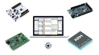
FPGA’s are everywhere with their presence in the diverse set of the domain is increasing day by day. The two most popular Hardware description languages are VHDL and Verilog each having its unique advantage over the other. The best part about both of them is once you know one of them you automatically understand the other and then the capabilities of both worlds can be used to build complex systems. The course focus on the Verilog language. The curriculum is framed by analyzing the most common skills required by most of the firms working in this domain. Most of the concepts are explained considering practical real examples to help to build logic.
The course illustrates the usage of Modeling style, Blocking and Non-blocking assignments, Synthesizable FSM, Building Memories with Block and Distribute Memory resources, Vivado IP integrator, and Hardware debugging techniques such as ILA and VIO. The course explores FPGA Design flow with the Xilinx Vivado Design suite along with a discussion on implementation strategies to achieve desired performance. Numerous projects are illustrated in detail to understand the usage of the Verilog constructs to interface real peripheral devices to the FPGA. A separate section on writing Testebench and FPGA architecture further builds an understanding of the FPGA internal resources and steps to perform verification of the design.
Who this course is for:
- VLSI Job Seeker/ Graduate student looking to pursue career as RTL Engineer/ Design Engineer/ Verification Engineer.
- Anyone interested to learn Xilinx FPGA/ Vivado Design Suite/ Verilog Hardware Description Language
- Anyone interested to start career in ASIC/ VLSI domain.
User Reviews
Be the first to review “Verilog for an FPGA Engineer with Xilinx Vivado Design Suite”
You must be logged in to post a review.


There are no reviews yet.